Tower’s $3 Billion Japan Bet Is About Wiring AI, Not Building Another Logic Megafab
With METI support, Tower is expanding 300mm silicon photonics, SiGe, and advanced packaging in Japan on two tracks, one aiming for production readiness in late 2027, the other a new fab beside Uozu that still depends on closing deals.
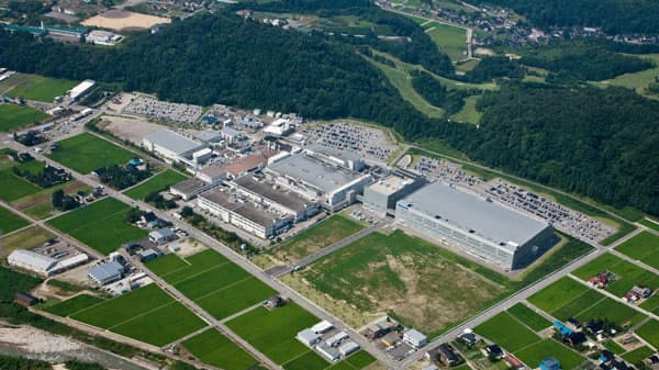
AI clusters do not only need leading-edge logic wafers. They also need optical links that can move data between accelerators, switches, and memory without burning the power budget. On July 14, 2026, Tower Semiconductor and Japan’s Ministry of Economy, Trade and Industry put that quieter bottleneck on the industrial map: a dual-track expansion of 300mm silicon photonics, silicon germanium, and advanced packaging in Toyama and Niigata, with METI certification the same day.
Tower’s English release frames the dual-track scope as roughly three billion dollars of company investment, net of about one billion dollars in Japanese government grants. METI’s yen framing for the certified supply-assurance plan puts project investment around six hundred billion yen, with ministry support of up to about one hundred sixty billion yen. Those figures describe a planned build, not cash already spent, and Tower’s own forward-looking statements warn that grant terms and covenants can put a portion or all of grant funds at risk.
Track One is the near-term executable piece. Tower plans to repurpose the Arai facility in Myoko, Niigata, formerly Fab 6, for 300mm silicon photonics and advanced packaging, while maximizing 300mm output at Fab 7 in Uozu, Toyama. Full production readiness for that track is expected in the fourth quarter of 2027. Tower says it is updating its business model to target 3.6 billion dollars of revenue and 1.2 billion dollars of net profit in 2028 based on Track One’s growth outlook. Those 2028 numbers are company targets, not audited results and not a METI guarantee. Tower’s investor FAQ is explicit that the updated model rests solely on Track One.
Track Two runs in parallel on paper and later in concrete. It calls for constructing an additional 300mm manufacturing facility adjacent to Fab 7 after related agreements are signed and closed. Tower expects that site to multiply silicon photonics and silicon germanium capacity for AI and data-center optical connectivity, with accretion language pointed at 2029 and beyond. Until definitive agreements close, treat Track Two as contingent upside rather than a groundbreaking date you can put on a calendar.
Japan’s policy frame matters as much as the tool install schedule. Semiconductor supply assurance under the Economic Security Promotion Act is the architecture behind METI’s certification, including multi-year production obligations after supply starts. Minister Ryosei Akazawa’s remarks the same day placed the plan in photonics-electronics convergence and expected domestic collaboration, including with NTT: an expectation, not a disclosed Tower customer contract in the July 14 company release. Capacity start dates and wafer volumes published in secondary summaries of METI plan materials should be rechecked against the ministry overview before anyone treats them as frozen.
Readers who already followed TSMC’s Arizona megafab story will recognize the subsidy muscle and miss the technology layer if they stop there. Arizona is a leading-edge logic and packaging campus story. Tower’s Japan bet is a specialty analog foundry multiplying the optical interconnect processes that sit beside those accelerators. Uozu already ships advanced silicon photonics flows; Arai’s return and a possible adjacent fab are about scale, not inventing the category from scratch.
The next checkpoints are concrete. Watch for definitive agreements and groundbreaking language on Track Two, the April 1, 2027 TPSCo restructuring close that Tower has described separately, and whether fourth-quarter 2027 readiness holds as tools land. Toyama and Niigata are not abstract “ecosystem” words here. They are the prefectures where Japan is paying to keep optical manufacturing capacity onshore while AI demand keeps raising the bandwidth bill.
Optical SiPho and SiGe capacity is a distinct AI bottleneck from leading-edge logic, and Tokyo just put subsidy muscle behind it.
Related stories
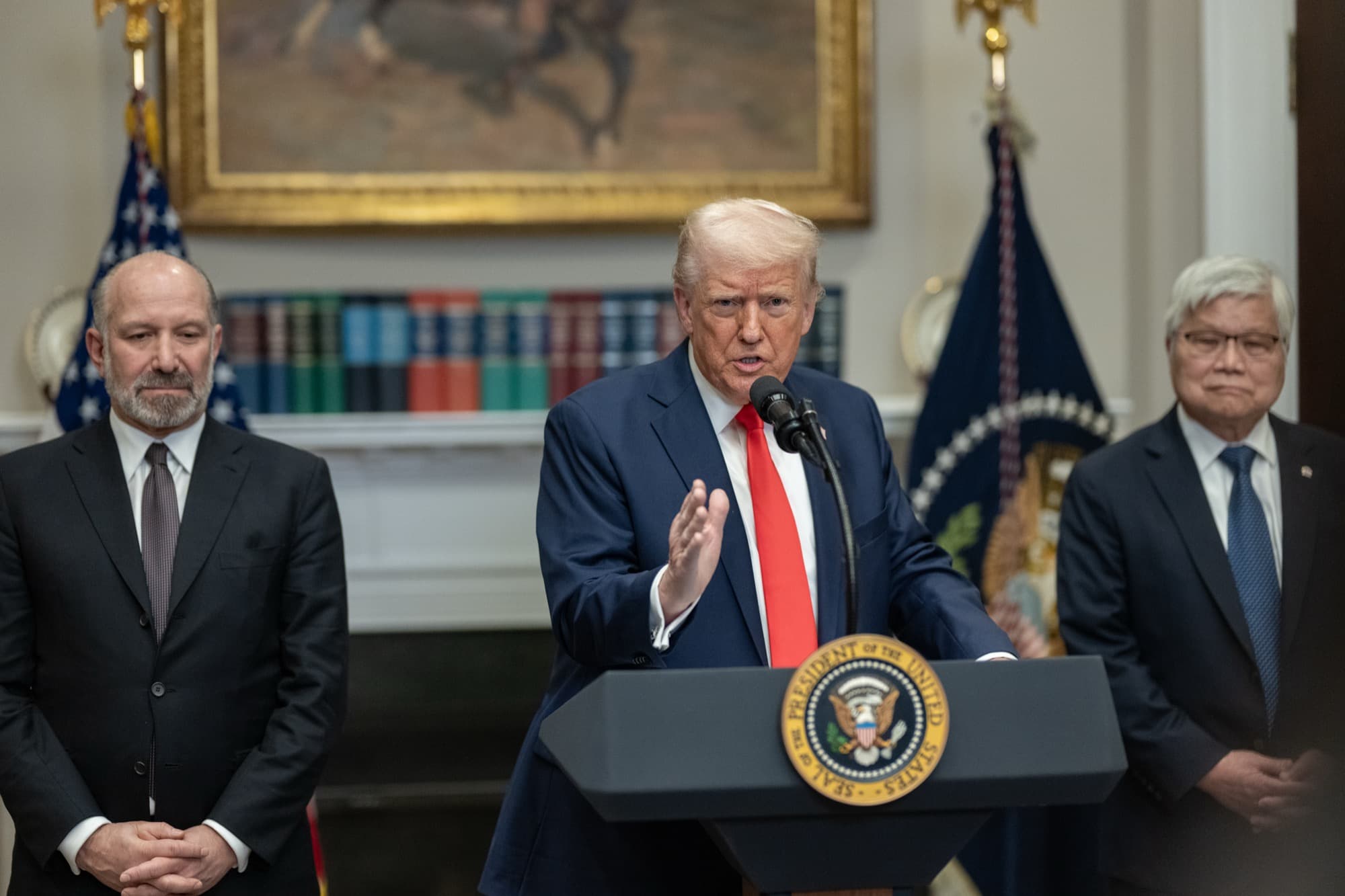
TSMC’s $265 Billion Arizona Bet Is Really About Packaging the AI Boom
On its July 16 earnings call, TSMC tied a fresh $100 billion Arizona commitment to packaging capacity so tight it is limiting customers’ growth.
4 min · Jul 16, 2026
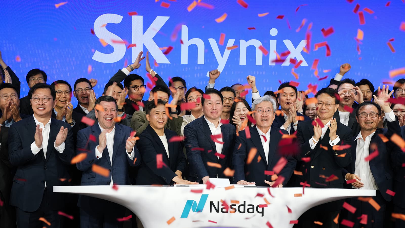
Why SK hynix Shares Are So Volatile After Its Nasdaq Debut
SKHY and Seoul-listed 000660 represent the same chipmaker, but July’s listing structure briefly made them look like different stories.
7 min · Jul 16, 2026
DHL’s Bangkok–Cincinnati Freighter Maps the New Asia–U.S. Air Cargo Story
A thrice-weekly Bangkok–Cincinnati freighter with up to 100 tons per flight shows how AI and semiconductor hardware are reshaping Asia–U.S. air cargo.
4 min · Jul 9, 2026

AI Hardware Is Filling Transpacific Air Cargo to the Ceiling
Xeneta puts Asia–North America dynamic load factors at 90%. May Taiwan–U.S. rates hit $7.02 per kilo. Korean Air’s cargo yield jumped about 42% in the second quarter.
5 min · Jul 24, 2026